Flash memory has become ubiquitous in our modern digital world. The memory storage technology powers your smartphone, USB thumb drive, digital camera’s SD card, and even solid-state (SSD) in your new laptop. Its characteristics, such as non-volatility, high density, and low power consumption, make it a favored storage medium. But how exactly does flash memory work? This article aims to explain the operation of flash memory in simple terms.
How Does a Flash Memory Work?
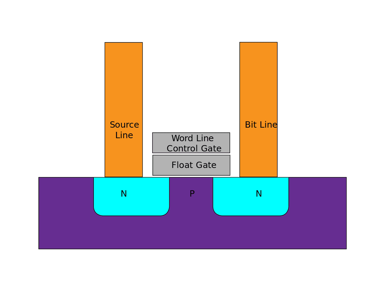
- Flash Memory Components: Flash memory comprises an array of cells made from floating-gate transistors. The floating gate can be conductive (like polysilicon) or non-conductive (as in SONOS flash memory).
- Single-Level Cell (SLC) and Multi-Level Cell (MLC): SLC devices store one bit of information per cell, while MLC devices (including triple-level cell (TLC) devices) can store more than one bit per cell.
- Floating-Gate MOSFET: Each memory cell resembles a standard metal–oxide semiconductor field-effect transistor (MOSFET) but has two gates instead of one: a control gate (CG) and a floating gate (FG). An insulating oxide layer electrically isolates the FG.
- Data Writing: Data is written to flash memory by charging the FG with electrons, which increases the cell’s threshold voltage (VT). This voltage can change between an uncharged FG threshold voltage (VT1) and a charged FG threshold voltage (VT2).
- Data Reading: Data is read from the memory cell by applying an intermediate voltage (VI) between VT1 and VT2 to the CG. If the channel conducts at VI, it means the FG is uncharged (representing a ‘1’); if not, it means the FG is charged (representing a ‘0’).
- MLC Operation: In MLC devices, the precise amount of current flow is detected to determine the charge level on the FG more accurately, as these devices store more than one bit per cell.
- Endurance and Degradation: Over time, the high electric field experienced by the oxide layer can cause degradation, leading to electron leakage, which increases the risk of data loss. Each erase operation also contributes to this degradation.
- Cell Retirement: To maintain performance and reliability, degraded cells that have accumulated too much negative charge and are slow to erase must eventually be retired.
- Influence of Bit Number: The number of bits stored in a cell affects its endurance. More bits mean more possible states and sensitivity to programming voltages, requiring careful adjustments to maintain reliability as the silicon oxide layer degrades.
Flash memory, a cornerstone of modern digital storage, relies on an array of memory cells composed of floating-gate transistors. The intricacies of its operation are even more fascinating when considering single-level cell (SLC) and multi-level cell (MLC) devices, including triple-level cell (TLC) devices. This article takes a deep dive into the operations of these memory devices, explaining how they store data and why wear and tear happens over time.
SLC vs. MLC
In an SLC device, each memory cell stores one bit of information. It’s simple and straightforward and offers high performance and longevity. On the other hand, MLC devices, including TLCs, store more than one bit of information per cell. The floating gate of these memory cells can be conductive (like polysilicon) or non-conductive (as seen in SONOS flash memory).


The Floating-Gate MOSFET
In essence, each memory cell in flash memory is akin to a standard metal–oxide semiconductor field-effect transistor (MOSFET), except it features two gates instead of one: a control gate (CG) and a floating gate (FG). The FG, electrically isolated by an oxide layer, can hold electrons. When charged with electrons, this FG effectively screens the electric field from the CG, thus modifying the cell’s threshold voltage (VT). Depending on the FG charge, this threshold voltage can fluctuate between an uncharged FG (VT1) and a higher-charged FG (VT2).
Reading Data from Flash Memory
An intermediate voltage (VI) between VT1 and VT2 is applied to the CG to read a value from the cell. If the channel conducts at this voltage, the FG must be uncharged. If it doesn’t, the FG is charged. In a binary system, this differentiation enables the storage of information.
In multi-level cells, where more than one bit per cell is stored, the presence or absence of current flow does not matter; it’s the amount. The quantity of current flow allows for more precisely determining the FG’s charge level.
Floating Gate Endurance and Degradation
The floating gates are named such because an electrically insulating tunnel oxide layer separates them from the silicon, causing the gate to “float” above the silicon. This oxide layer keeps the electrons confined within the floating gate.
However, the high electric field experienced by the oxide (up to 10 million volts per centimeter) can cause atomic bond breaks over time, gradually degrading the oxide’s electrically insulating properties. Over time, this can lead to electrons being trapped in or freely passing (leaking) through the oxide from the floating gate, increasing the risk of data loss.
Moreover, each erase operation further degrades the silicon oxide within a cell. This cumulative degradation increases the cell’s negative charge due to trapped electrons, negating some control gate voltage and slowing the cell’s erase process. These degraded cells must eventually be retired to maintain the NAND chip’s performance and reliability.
The number of bits in a cell directly affects its endurance. With more bits, the number of possible states, represented by different voltage levels, increases, making the cell more sensitive to programming voltages. As the number of bits increases, there’s less tolerance for adjustments to these voltages due to the reduced space between voltage levels defining each state in a cell. Thus, careful voltage adjustment becomes necessary to compensate for the degradation of the silicon oxide.
At the most fundamental level, flash memory is a type of Electrically Erasable Programmable Read-Only Memory (EEPROM). It stores information in an array of memory cells made from floating-gate transistors. In simple terms, each transistor acts as a switch that can either block or allow the flow of electricity, representing binary states—1 or 0.
The critical component of these transistors is a specially designed gate, known as a ‘floating gate,’ trapped between two other layers (control gate and substrate). This floating gate can hold an electrical charge. Depending on whether a charge is held or not, we can use this to represent our binary data states.
Writing Data
An electric charge is sent through the specific memory cell’s control gate to write data into the flash memory. This process uses a high voltage to force electrons through the insulating barrier onto the floating gate, a process known as ‘tunneling.’ Once this charge is in place on the floating gate, it’s isolated and ‘trapped’ there by the insulating layers. The presence of this charge is used to represent a ‘0’ in binary language.
In contrast, if the floating gate is free of charge, this condition represents a ‘1.’ This differentiation between the charged and non-charged state of the floating gate allows flash memory to store binary data (a series of ones and zeros), which can be translated into any form of digital content, like photos, videos, text files, etc.
Erasing Data
Another high-voltage charge is applied to erase data from memory, this time to the substrate or bottom layer of the transistor. This charge effectively pulls the electrons off the floating gate through the same tunneling effect but in the opposite direction, thus erasing the data stored in that cell.
Storage and Durability
One significant benefit of flash memory is that it is non-volatile. This means that once data is written to the memory, it doesn’t need a constant power supply to maintain the information. Even when you switch off your digital device, the data stays intact.

However, this process of writing and erasing by forcing electrons to tunnel through the insulating oxide layer leads to gradual wear and tear. After many write/erase cycles, the insulating layer starts to break down, which can eventually result in the memory cell failing. The number of cycles a flash memory cell can handle before failure is variable. Still, it’s typically in the tens or hundreds of thousands, which is generally more than sufficient for many consumer devices.
In Conclusion
Flash memory relies on the movement and trapping of electrons to write, store, and erase data. Its design allows for high-density, non-volatility, and relatively low power usage, making it a cornerstone of modern digital storage. Despite its limitations in write/erase cycles, technological advancements continue to improve its durability and capacity, ensuring that flash memory will play a vital role in our digital world for the foreseeable future.


Learn more about authors in Nimblefreelancer's team biography page.
- 6 Proven Ways SaaS Founders Actually Get Customers (With Real Examples) - December 17, 2025
- Facebook Ads to Get Followers! - December 27, 2024
- ClickUp vs. Slack - December 20, 2024